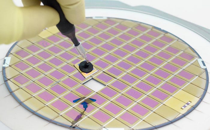
Wafer Coring Services
Wafer coring involves reducing the diameter of the wafer so that it fits into the available processing equipment. This helps to ensure that the wafer can be properly processed and inspected.
We offer wafer coring services on silicon, alumina, piezoceramics, glass and layered combinations of materials. These processes involve die singulations on wafers but also cutting grooves and forming surface features.

Resizing
Resizing is the process of reducing the size of a wafer so that it fits into the available processing equipment. It is a cheaper solution than replacing expensive tooling, and it will also ensure that your process yields are high.
Resizing involves cutting a wafer to a smaller diameter, usually using laser technology. This is a more flexible alternative to mechanical sawing, and it is less damaging to the surface of the wafer.
In some cases, resizing a wafer can be as simple as removing a flat or notch from a larger wafer. This helps keep the orientation of the grain in the wafer and maintains alignment during processing.
Crystal Mark offers laser resizing services that use a Synova tool to direct the laser to the wafer’s cutting path. This resizing method creates a cut that is minimally damaged near the ablation point, and with very straight sidewalls. It is ideal for coring and resizing silicon, sapphire, geranium, GaAs, NaG, and other III-V materials.
Dicing
Dicing is the process of dividing a wafer so that it fits into the available processing equipment. It’s an essential step for producing microelectronic devices, such as microprocessors and memory chips.
Dicing involves the use of abrasive blades that rotate with a spindle at high speeds (usually 30,000–60,000 rpm). These dicing blades comprise diamond grit embedded into an electroplated nickel matrix, which is designed to crush the substrate material and remove debris.
The blade moves between active areas of the dice through dedicated dicing lines called streets, creating grooves in the wafer material.
There are several different dicing methods, including blade dicing and plasma dicing. The blades used for each method have their own advantages and disadvantages.
One of the most common methods of dicing is wax mounting, which improves bottom-side support and reduces backside chipping. However, this process is time-consuming and requires manufacturers to clean the workpieces before the dicing begins. Some companies use tape to mount the substrates, which can also result in fewer instances of chipping.
Polishing
Polishing is the process of removing surface imperfections on a material. This can be done with a variety of abrasives and dry polishing materials.
Chemical mechanical polishing (CMP) is a method that combines chemicals and physical abrasion to remove material on a semiconductor wafer. The chemical component reacts with the surface and causes it to become smoother, while the mechanical part removes the material through physical abrasion.
CMP is used to remove a layer of roughness on a semiconductor wafer’s surface to produce a mirror-like finish. The process also reduces the amplitude of dopant striations.
The polishing of a wafer can be accomplished by using a single-sided or double-sided polisher. In the case of a single-sided polisher, the wafer is mounted on an arm and moved around on a ceramic turntable to a polished surface.
Thinning
Thinning is a stage in the semiconductor manufacturing process that reduces the thickness of a wafer. This helps to create ultra-thin chips for more advanced integrated circuits.
The process begins with a mechanical grinding technique. This involves a grinding tool that contains diamond particles of specific dimensions.
For this to occur, a wafer is positioned on a porous ceramic rotating vacuum chuck with its backside facing the grind wheel. The chuck and grind wheel rotate in opposite directions while deionized water is sprayed onto the work piece to provide cooling and wash away material particles that came off during the grind.
The backside of the wafer is thinned using a mechanical grinding method that consists of coarse and fine grinding steps. The coarse grind removes a large amount of silicon from the back side, significantly reducing its thickness.
